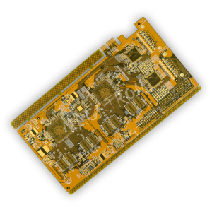
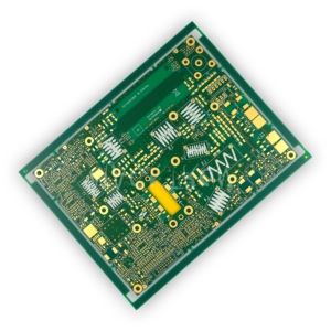
RF & Microwave PCB
Layer Count: 8
Layer Count: 8
Thickness: 1.00 mm
Min. Hole: 0.2 mm
Aspect Ratio: 5:1
Min. Trace/Space: 4.10/7.80 mil
Additional Features:
L1-4 & L5-8 Blind vias
2 pressing cycles
2 Resin Fill cycles
S1000-2M & RO4350B composite
Controlled impedance

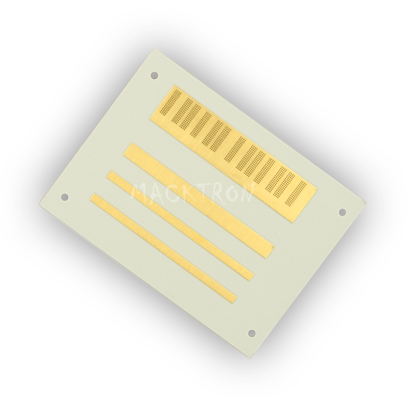
RF & Microwave PCB
Layer Count: 2
Layer Count:2
Thickness:0.15 mm
Panel Size: 76.00 * 44.00 mm
Additional Features:
Soft gold
RO4350B substrate
Selective 78.74u” gold

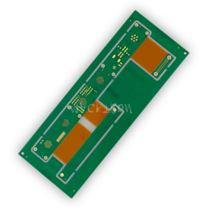
RF & Microwave PCB
Layer Count: 2
Layer Count: 2
Thickness: 1.60 mm
Min. Hole: 0.20 mm
Aspect Ratio: 8:1
Min. Trace/Space: 0.10 mm
Surface Finish: ENIG
Additional Features:
RO5880 material
Application: telecommunication

RF & Microwave PCB
Layer Count: 8
Layer Count:8
Thickness:1.10 mm
Min. Hole: 0.2 mm
Aspect Ratio: 5.5:1
Min. Trace/Space:7.87/5.80 mil
Additional Features:
L1-L7 Blind via
2 pressing cycles
2 Resin Fill cycles
IT180a & RO4350B composite
Soft gold
Selective 40u” gold

RF & Microwave PCB
Layer Count: 12
Layer Count:12
Thickness:1.50 mm
Min. hole: 0.2 mm
Aspect Ratio: 7.5:1
Min. Trace/Space:3.90/5.90 mil
Additional Features:
L1-L10 Blind via
2 pressing cycles
2 Resin Fill cycles
S1000-2M & RO4350B composite
Soft gold
Selective 40u” gold
PTH Slot Holes

RF & Microwave PCB
Layer Count: 2
Layer Count:2
Thickness:0.15 mm
Panel Size: 92.50 * 100.00 mm
Additional Features:
Soft gold
Selective 78.74u” gold
Rogers RO5880 Substrate

RF & Microwave PCB
Layer Count: 2
Layer Count: 2
Thickness: 1.60 mm
Min. Hole: 0.20 mm
Aspect Ratio: 8:1
Min. Trace/Space: 0.10 mm
Surface Finish: ENIG
Additional Features:
PTFE Material
Application: telecommunication
RF & Microwave PCB
Layer Count: 2
Layer Count:2
Thickness:0.31 mm
Panel Size: 53.95 * 73.09 mm
Additional Features:
ENEPIG
RO4350B Substrate
Application: remote controller