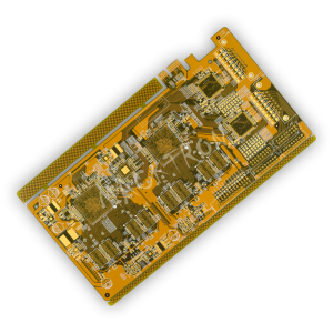
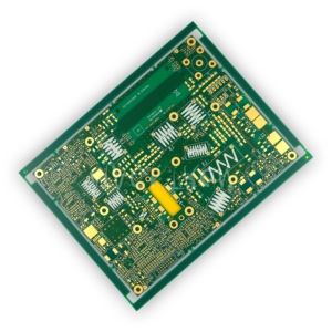
Multi-layer boards combine the basic single and double sided boards to increase the wiring spaces. A layer of insulation was placed between each level and the layers are laminated together. Technically, Multi-layer boards can comprise 4 to 60 layers or more. The primary technology is the precise positioning between the layers as well as the control and handling of the thick and heavy boards throughout the production process.
According to estimations made by Prismark, Multi-layer boards accounted for 35% of the total gross output (US$57.5 billion) for PCB in 2014, which accounted for the biggest portion in the technology category. The average compound annual growth rate for multi-layer boards between 2013-2018 is estimated at 2.1%. The products are widely used in computing, telecommunications, consumer, automotive, industrial, medical, military, aerospace, and other products.
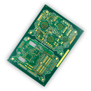
High density interconnect (HDI) boards primarily adopt the micro-blind/buried hole technology to make PCBs with higher density circuits. The largest difference between a HDI and a traditional PCB is the hole formation method. HDI technology adopts the non-mechanical drilling method that primarily uses laser drills. In addition, HDI adopts additive layer method. As the number of the layers increases, the corresponding technological capacities are elevated as well. Advanced circuit board technologies such as electrolytic hole filling, hole stacking, and direct laser drilling are adopted during the production process.
HDI boards have the advantages of being lightweight, thin, short, and small as well as having higher line densities, better electrical characteristics and signals, short transmission path, and improvable radio frequency interference / electromagnetic interference / electrostatic discharge. Any-layer HDI is the high-end technology that uses laser drilling to open up connections between the layers, and thereby allowing the product to be lighter and thinner. The degree of difficulty for this technology is higher as well. According to estimations made by Prismark, HDI boards accounted for 14.6% of the total PCB gross output (US$57.5 billion) in 2014. The average compound annual growth rate for HDI boards between 2013-2018 is estimated at 3.4%. The products are widely used in smartphones, tablets, wearable devices, LCD panels, automotive, and storage devices.
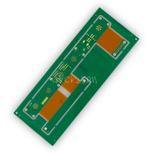
PCBs are generally divided into rigid and flexible types. When a flexible board is sandwiched between two rigid boards to structure a PCB, it is known as the Rigid Flex Board. According to different manufacturing processes, rigid-flex Boards can be classified as follows:
- Rigid flex board (99%) — Uses an entire flexible board as the base with the PP or core layer added on top and pressed-fit to create a PCB.
- Rigid flex combination board (1%) — Only the flexible board portion is produced, and then the flexible board is buried into the rigid board and pressed-fit into a PCB (presently patented by the Japanese manufacturer Ibiden).
The biggest advantage of a Rigid Flex Board is its lightweight, thinness, shortness, and smallness qualities. In addition to saving space, it can also effectively reduce the noise problems produced during signal transfers from the flexible board to the rigid board. Due to Rigid Flex Boards’ better reliability, signal integrity, noise suppression, and impedance control characteristics, they are widely adopted for smartphones, LCD panels, CMOS, battery modules, and wearable devices.
High-frequency Board has recently become a key focus of development because the flourishing developments of big data, wireless transmission, and social group networking have driven the popularity of electronic devices such as smartphones, tablet PCs, and notebook computers as well as increased the demands for high-speed electronic products/high-frequency networks.